Pressure induced metallization and superconductivity in the van der Waals compound CuP2Se – Dr. Hengzhong Zhang
NOVEMBER 24, 2021
A research team led by Dr. Hengzhong Zhang from the Center for High Pressure Science and Technology Advanced Research (HPSTAR) revealed that a new Cu-bearing van der Waals compound CuP2Se can be metallized and then turned into a superconductor accompanying a series of structural changes under compression. Their study illustrates that pressure can be used to harvest useful physical and chemical properties of Cu-bearing vdWs materials. These findings were recently published in the Journal of the American Chemical Society.
Layered van der Waals (vdW) materials have tunable properties for developing novel catalysts, optoelectronic devices, photodetectors, sensors, etc. Layered Cu-bearing compounds is a new family of the vdW materials, whose structures and properties, especially the potential superconductivity, are yet to be studied.
“Different methods can be used to modulate their interlayer coupling to produce desirable properties in the van der Waals materials,” said Dr. Zhang. “Pressure has been a quite unique tool in tuning the physical properties of materials”. “So how pressure would work on the Cu-bearing vdW materials was the most we wanted to know in this study.”
The team led by Dr. Zhang set out to use multiple state-of-the-art experimental techniques and theoretical calculations to map structural changes as well as potential superconductivity in CuP2Se, a model compound with relatively simple chemical composition and crystal structure.
By doing this, the scientists found that through pressure tuning of the interlayer coupling, CuP2Se experienced a series of structural changes, such as two isostructural changes at ~10 and 20 GPa, respectively. At even high pressure, the CuP2Se sample went through a transition from a vdW phase to a high-coordination phase.
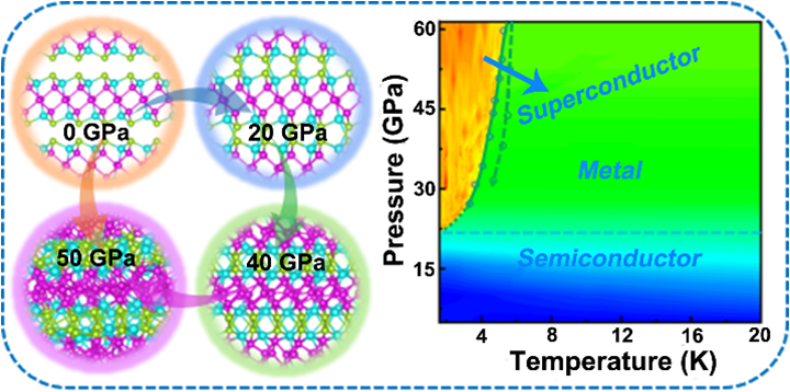
Of particular interest is that these structural changes induced a semiconductor-to-metal transition at ~ 20 GPa at room temperature, and a metal-to-superconductor transition at low temperatures and at higher pressures.
To better understand the enhancement in the critical superconducting temperature, the team carried out BCS-theory modeling. They found that the increase in the critical temperature at high pressure originated primarily from the enhancements in the bulk modulus and the electron density of states at the Fermi energy.
“Our findings will have important implications to the development and applications of layered vdWs materials in electronic devices and sustainable energy,” said Dr. Zhang.
Caption: Structural changes at high pressure (left) and superconducting phase diagram (right) of the van der Waals compound CuP2Se.
层状范德华(vdW)化合物在电催化、锂电池、电子和光电子器件等领域具有广泛的应用前景。最近发现的铜基层状化合物是一类新的范德华化合物,但其诸多物性,如潜在的超导电性,依然未知。最近,北京高压科学研究中心张衡中博士领导的研究组利用多种原位高压实验技术和理论计算研究了层状化合物CuP2Se在高压下的结构演变以及其光学和电学等性质的变化。他们发现,CuP2Se在~10 GPa & 20 GPa,经历了两个同构相变,在更高压力,CuP2Se又由范德华相转变成了高配位相。并且,伴随这些晶体结构的变化,半导体的CuP2Se在~20 GPa转变成了金属,随着压力的进一步增加,又由金属转变成了超导体并且超导转变温度伴随压力的增加而升高。通过BCS理论模拟,他们发现该化合物超导临界温度伴随压力的升高主要归因于高压下体弹模量的增加和费米能处电子态密度的增加。相关的研究成果以 “Metallization and Superconductivity in the van der Waals Compound CuP2Se through Pressure-Tuning of the Interlayer Coupling”为题发表在《美国化学会志》上。