Pressure engineered Sb2S3 for better semiconductors – Dr. Qingyang Hu
SEPTEMBER 2, 2021
Semiconductors were widely used in manufacturing chops, solar cells, photovoltaic devices and so on, which have defined the third industrial revolution since the late 1900s. Although a large number of semiconductor materials are in production, people are still seeking new semiconductor materials with higher energy conversion efficiency. Choices for environmentally friendly and affordable semiconductors are limited. However, it is possible to optimize the properties of semiconductor materials through doping, preparing thin films, and high-temperature annealing. Here, we introduce an effective, energy-efficient and pollution-free approach to continuously modulate the band gap of Sb2S3 at gigapascal pressures by means of hydrostatic pressure compression. The research is published in Communications Chemistry.
One of the most important parameters for semiconductor is its band-gap energy, which will determine its field of implication. Sb2S3 is a typical transition metal sulfide, with a favorable band-gap energy of 1.5eV~2.2eV for solar energy conversion. It features a wide response range to the solar spectrum and has higher conversion efficiency than single-crystal silicon in absorbing near infrared light. With good Earth abundance and tolerance to high temperature, Sb2S3, or the mineral stibnite, makes a promising material for photoelectric and potentially a thermoelectric material which converts heat to controllable energy. The only drawback of Sb2S3 is its band-gap energy is slightly higher than the optimal band gap value of 1.5 eV for the absorber layer of solar cells, which reduces the efficiency of its absorption of sunlight.
Our group reported a novel form of bulk Sb2S3 samples by breaking its ambient layered structure using pressure. We applied external stress to squeeze the Sb2S3 layer supported by the weak van der Waals forces. This method is the opposite way of manufacturing graphene, which breaks van der Waals carbon layers by striping graphite. Instead, we attached those layers together and enforced them to form stronger covalent bonds. This 3D structure of Sb2S3 features lower bandgaps upon the structural transformation at gigapascal pressures.
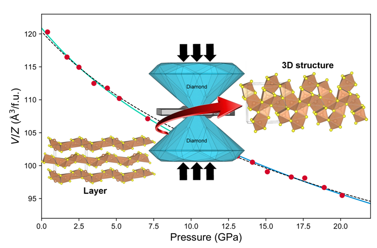
Applying external stress has renovated both the crystal and electronic structure of Sb2S3. Raman spectroscopy is sensitive to the chemical bonds and the evolution of Raman under compression suggest a large number of soft interlayer bonds disappear and was replaced by rigid interatomic bonds near the transition pressure. This is also consistent with other structural probes like x-ray diffraction and computational simulations. Moreover, during the pressurization process, the band gap of Sb2S3 transforms from the indirect band gap type to the direct band gap type, which will shorten the recombination lifetime and improve photovoltaic properties. We found the phase transition is irreversible if pressure was removed. This means that even Sb2S3 returned to atmospheric pressure, it still maintains the compact 3D structure. This property opens up the possibility of designing semiconductor devices using 3D-Sb2S3.
Our experiment is among the many examples of showing pressure as an effective means of modulating material properties. Compressed structure can engineer electronic structures and design better materials for industrial implications.
Caption: Pressure induced structure and bandgap change in Sb2S3.
压力可以使层状的石墨转变为坚硬的金刚石,类似的层状结构到体材料的相变通过高压可以普遍实现,并且能对材料的能带结构进行调节。高科的崔中迅和胡清扬领导的实验小组通过施加压力破坏了层状辉锑矿(Sb2S3)中的范德华力,形成了一种新的块状辉锑矿晶体。 辉锑矿在十万个大气压的压力下转变三维结构,其具有较低的带隙,并且这种相变在撤去压力后不可逆的。这意味着三维辉锑矿仍然保持这种紧凑结构,即使恢复到常压。利用这一特性可以设计基于窄能带辉锑矿的高性能半导体器件器件。我们的实验展现了压力可以作为一种调节材料特性的有效手段,施加压力可以为设计更好的材料提供一种新的途径。