A new two-dimensional carbon allotrope — semiconducting diamane film synthesized - Dr. Feng Ke,Lingkong Zhang & Dr. Bin Chen
JUNE 25, 2020
Atomically thin diamond, also called diamane, is a two-dimensional carbon allotrope and has attracted considerable scientific interest due to its potential physical properties. However, previous studies suggest that atomically thin diamond films are not achievable in a pristine state because diamonds possess a three-dimensional crystalline structure and would lack chemical stability when thinned down to the thickness of diamond's unit cell due to the dangling sp3 bonds. Chemical functionalization of the surface carbons with specific chemical groups was considered necessary to stabilize the two-dimensional structure, such as surface hydrogenation or fluorination, and various substrates have also been used in these synthesizing attempts. But all of these attempts change the composition of diamond films, that is to say, the successful synthesis of a pristine diamane has up until now not been achieved.
Regulating the phase transition process of carbon materials under high pressure and high temperature is always a straightforward method for achieving diamondization. Here, a team of scientists led by Drs. Feng Ke and Bin Chen from HPSTAR (the Center for High Pressure Science and Technology Advanced Research) used this direct approach, diamondization of mechanically exfoliated few-layer graphene via compression, to synthesize the long-sought-after diamane film. The study is published in Nano Letters.
The diamondization process is usually accompanied by an opening of an energy gap and a dramatic resistance increase due to the sp2−sp3 rehybridization between carbon atoms. “The in-situ electrical transport measurements of few-layer graphene are difficult to carry out under high pressure,” said Feng Ke “However, using our recently developed photolithography-based microwiring technique to prepare film electrodes on a diamond surface for resistance measurements, we are able to study the pressure-induced sp2−sp3 diamondization transition of mechanically exfoliated graphene with layer thickness ranging from 12- to bilayer at room temperature.”
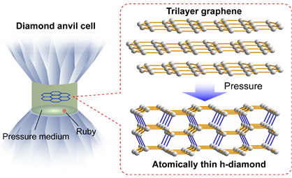
Caption: pressure-induced graphene-diamane transition.
Their studies demonstrate that pristine h-diamane could be synthesized by compressing trilayer and thicker graphene to above 20 GPa at room temperature, which once synthesized could be preserved to ∼1.0 GPa upon decompression. “The optical absorption reveals that h-diamane has an energy gap of 2.8 ± 0.3 eV, and further band structure calculations confirm an indirect band gap of 2.7−2.9 eV,” explained the co-frist-author Lingkong Zhang, a PhD student at HPSTAR. “Compared to gapless graphene, semiconducting h-diamane offers exciting possibilities for carbon-based electronic devices.”
The XRD measurements have shown that the few-layer graphene to h-diamane transition is a gradual structural transition, which helps to understand the continuous resistance increase and absorbance decrease in trilayer and thicker graphene with pressure above the transition pressure. Theoretical calculations indicate that a (−2110)-oriented h-diamane is energetically stable and has a lower enthalpy than its few-layer graphene precursor above the transition pressure.
“Like the discovery of graphene, carbon nanotubes, fullerenes, and other novel carbon allotropes, the realization of a pristine diamane represents another exciting achievement in materials science,” added Dr. Bin Chen, “Thermal treatment at high pressure may be helpful to preserve a pristine h-diamane to ambient pressure, as suggested from the high-temperature and high-pressure method to synthesize a pressure quenchable h-diamond. The challenges still remain to achieve the preservation and industrial applications of diamane.”
石墨烯的零带隙性质严重制约着其在高性能场效应管方面的应用。合成具有高载流子迁移率且合适带隙的新型二维材料成为了材料科学家们孜孜追求的目标。近期,与石墨烯为同素异形体的钻石烯,即将钻石(金刚石)减薄至原子层级别的新型碳材料引起了人们的广泛关注。截至目前,科学家们通过表面钝化处理,比如表面碳原子氢化、氟化、加入其他官能团等方式已成功制备出立方形的钻石烯材料。而表面钝化处理必然会对材料的载流子迁移率产生较大影响,并且这种方式合成的主要是具有较宽带隙的立方形钻石烯。北京高压科学研究中心的柯峰博士及其合作者通过高压调控技术,成功合成(-2110)型六方钻石烯材料,其带隙约为 2.8 eV。这种新型钻石烯材料的体内碳原子为sp3成键,但是表面的碳原子仍然部分保留了sp2成键,使得其带隙远低于金刚石的带隙(~5.6 eV)。由于表面sp2成键的存在,钻石烯可能也具有很高的载流子迁移率。这一新型二维材料的合成为制备高性能碳基场效应管提供重要指导。相关研究以“Synthesis of Atomically Thin Hexagonal Diamond with Compression”为题发表于Nano Letters。