Pressure-induced inverse photoconductance in WO3/CuO heterostructure - Dr. Lin Wang
AUGUST 15, 2019
New study from a team of scientists led by Dr. Lin Wang of HPSTAR find pressure can effectively tune the photoreponses of nano heterojunction. They found a reversible inverse photoconductivity transition in WO3/CuO heterostructure under high pressure. Their study may provide an applicable tool with enhanced performance for photovoltaic devices, functioning as a switch, controller, or a potential light absorber and especially solar water splitting and solar degradation of organic pollutants in future. The study is published in recent Advanced Science.
It’s well-known that for most semiconductors, light will make it more conductive which is called positive photoconductivity. But in recent years, scientists found that in some special semiconductors, light can have the opposite effect — the electrical conductivity decreases with irradiation instead, which is called negative or inverse photoconductivity (IPC). IPC is a unique photoresponse behavior that just exists in a few materials, which has great potential applications in the development of photonic devices and nonvolatile memories with low power consumption. So scientists are trying to find more inverse photoconductors using multiple methods.
The team led by Dr. Lin Wang of HPSTAR utilized pressure to tune the photoresponse of a WO3/CuO heterostructure which is made of nano p-type WO3 nanocuboids and n-type CuO nanoparticles.
“Heterostructured materials made from wide and narrow bandgap semiconductors have more flexibilities in tuning the photoresponse and thus achieving the desired properties,” said Dr. Lin Wang. “While pressure is an effective tool in altering the physical properties of materials by tuning their lattice parameters, electronic structures, and electron–phonon coupling etc.
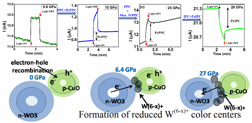
At relative lower pressures (below 6.4 GPa), the electrical conductivity of WO3/CuO heterostructure increase with pressure. When the pressure is increased to above 10 GPa, the sample exhibits persistent photoconductivity — the photoconductivity remains for a while even after the light is removed. After slightly increasing the pressure and switching on the laser, they observed that the conductivity becoming decreasing with illumination, which means a positive to negative photoconductivity transition at 29 GPa, continuing up to the highest pressure of 35 GPa. Interestingly, such a change from PPC to IPC was reversible with decompression.
To probe the behind reason of the reversible photoconductivity transition in the sample, the team carried out Raman&absorption spectroscopy, and x-ray diffraction measurements on the sample.
“The transition in photoconductivity is mainly related to pressure-induced changes in the structure, bandgap, WO6 distortion, and the electron–hole pair recombination process,” explained Dr. Saqib Rahman the lead author of the study, a postdoc of Dr. Lin Wang’s group.
Caption: Pressure induced photoconductivity variations in WO3/CuO heterostructure and the formation of reduced W(6-x)+ color centers at hte interface between CuO and WO3 phases upon compression.
光电导效应是一种光照变化引起材料电导变化的基本物理现象。对于大多数半导体材料,在光的照射下由于会产生更多的自由电子,因而电导率会增强—此效应叫做正向光电效应。然而近几年人们在少量的半导体材料中发现了负向的光电效应—电导率随着光的照射而减小。由于负光电导相对于正光电导在低能耗、高频率响应光电器件等领域也展现出了重要的应用前景,因而也受到了广泛的研究关注。北京高压科学研究中心的王霖研究员带领的研究小组使用高压的方法在WO3/CuO纳米复合材料中发现正向光电效应在一定压力下会转变为反向光电效应。并且当压力恢复到常压,反向光电效应又会转变为正向光电效应。该研究表明压力可以有效调节光电效应,并为设计新型光电探测器等提供了新的思路。